Surface analysis and material analysis
- Tandem time-of-flight secondary ion mass spectrometry (ToF-SIMS),
- X-ray photoelectron spectroscopy (XPS or ESCA),
- Atomic force microscopy (AFM),
- 3D-profilometry,
- Contact angle analysis (CA),
- ATR-FTIR analysis.
- Laser-induced breakdown spectroscopy (LIBS).
Equipment
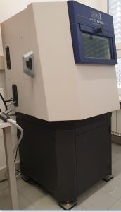
XPS device Kratos Supra+
X-ray photoelectron spectroscopy (XPS) is a surface analysis technique that determines the elemental composition and environment of an element ‒ i.e. its oxidation state and the chemical bond of the elements.
The Kratos Supra+ enables automatic angle resolved XPS measurements, the heating and cooling of the sample, and the depth profiling of organic matter using gas cluster ion beam (GCIB) technology and monoatomic argon ions.
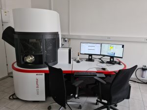
Kratos Supra+
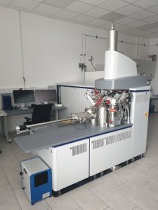
ToF-SIMS (MS/MS) IONTOF M6
Time-of-Flight Secondary Ion Mass Spectrometry, hereinafter: TOF-SIMS, is a surface analytical technique used to measure the mass spectrum on the surface of solids. The spectrometer enables high‑resolution analysis of elementary compositions and the molecular structure of surfaces, thin layers, and interphases of various materials (ceramics, semiconductors, polymers, biomaterials, coatings, etc.).
TOF-SIMS is a state-of-the-art device that enables high mass resolution, high spatial resolution, and depth profiling with dual beam ion sources, for both conductive and insulating materials.
The use of different ion sources allows the analysis of both inorganic and organic materials (especially in combination with the use of an Ar gas cluster ion source ‒ GCIB), thus obtaining high mass resolutions also for lighter elements such as hydrogen, nitrogen, and oxygen. Furthermore, high lateral resolution (<50 nm) in microanalysis and imaging can be acquired.
The device enables tandem (MS/MS) analysis, i.e. it is equipped with ToF/ToF analysers. Furthermore, it enables heating and cooling experiments, it is equipped with an EDR analyser, and Bi-LMIS, Cs/O2+, and GCIB ion sources.
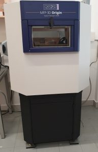
AFM device MFP-3D Origin AFM System (Asylum/Oxford Instruments)
An atomic force microscope (AFM) enables the study of topography at atomic resolution as well as interaction studies. It is applicable for the study of both conductive and non-conductive materials.
The equipment installed in our lab has the possibility of coupling with a potentiostat/galvanostat, enabling simultaneous electrochemical measurements while monitoring the topographic and morphological properties of the sample on the atomic scale.
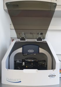
Profilometer DektakXT (Bruker)
A profilometer is an instrument that determines the profile of a sample by sliding the diamond tip stylus over its surface and recording the deviation from the reference plane of the sample, thus obtaining the data on surface roughness, the 3D-profile of the surface, as well as the thickness of the surface layer.
The device is used to examine different types of solid materials with a surface area of up to 10 cm in the x-direction and up to 10 cm in the y-direction. The latter complements atomic force microscopy (AFM) measurements, where the surface area of the measured sample is limited to 120 micrometres in the x-direction and 120 microns in the y-direction. Compared to AFM, a profilometer enables determination of topography of samples with a much larger height difference. However, the spatial resolution of the AFM instrument is higher.
Bruker’s DektakXT profilometer is equipped with 2 µm, 5 µm and 12 µm diameter stylus tips.
Contact angle analysis, OCA 25 (DataPhysics Instruments GmbH)
The optical contact angle measuring system OCA 25 is a measuring instrument for contact angle measurement and droplet shape analysis. The sample stage is adjustable in all three directions in space by means of a precision mechanism, allowing rapid manual sample adjustment. By capturing up to 3250 frames per second with a 6.5 x magnification lens and a high performance camera, even the fastest processes can be analysed. A single or double direct dosing system can be used for dosing liquids, as well as an electronic multiple dosing system. It is used to measure contact angles on absorbent surfaces such as cloths or powders.
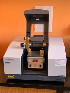
ATR-FTIR device, IRAffinity-1 (Shimadzu)
The attenuated total reflectance-Fourier transform infrared (ATR-FTIR) device is used to measure the infrared spectrum of samples without the need for extra preparation steps. An attenuated total reflection (ATR) module functions by measuring the changes that occur in an internally reflected infrared beam when the beam comes into close contact with a sample. For the technique to be successful, the refractive index of the ATR crystal must be greater than that of the sample.
ATR-FTIR is very useful for analysing thicker (compared to XPS and ToF-SIMS) surface layers of the sample in the solid state, sample drops, and different coatings. ATR-FTIR is widely used in the industry for the analysis of food products, biodiesel and other automotive fluids, pharmaceuticals, etc.
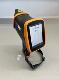
Laser-induced breakdown spectroscopy (LIBS; Vulcan EXPERT+, HITACHI)
Laser-induced breakdown spectroscopy is an analytical technique used for rapid elemental analysis of materials, where sample pretreatment is usually not required.
It is based on the generation of high-temperature plasma, which is formed by irradiating the sample with a focused short laser pulse. This causes ablation of the material and the transition of elements into an excited state. During relaxation from the excited to the ground state, the elements emit light at characteristic wavelengths, which are detected by the detector.
The typical limit of detection of the LIBS technique for heavy metal elements is in the parts-per-million (ppm) range. The technique has a wide range of applications, such as the analysis of alloys, semiconductors, glass, insulators, plastics, thin colour layers, electronic materials, etc.